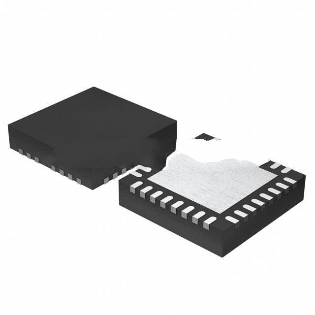
Brief introduction of MSP430G2553 microcontroller
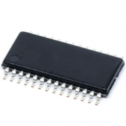
Brief introduction of MSP430G2553 microcontroller
1 MSP430 overview
• Low Supply Voltage Range: 1.8V to 3.6V
• Ultra-low power consumption
Run Mode: 230µA at 1MHz and 2.2V
Standby mode: 0.5μA
Off Mode (RAM Retention): 0.1μ
• 5 energy saving modes
• Ultra-fast wake-up from standby mode in less than 1μs
• 16-bit Reduced Instruction Set (RISC) Architecture, 62.5ns Instruction Cycle Time
• Basic clock module configuration
Internal frequency up to 16MHz with four calibration frequencies
Internal ultra-low power low frequency (LF) oscillator
32kHz crystal oscillator
External Digital Clock Source
• Two 16-bit Timer_A with three capture/compare registers each
• Up to 24 I/O pins with touch sensing support
• Universal Serial Communications Interface (USCI)
Enhanced Universal Asynchronous Transceiver (UART) with Auto-Baud Detection
IrDA encoder and decoder
synchronous SPI
I2C™
• On-chip comparator for analog signal compare function or slope analog-to-digital (A/D) conversion
• 10-Bit 200ksps Analog-to-Digital (A/D) Converter with Internal Reference, Sample-and-Hold, and Auto-Scan
• Brown-out detector
• Serial on-board programming without external programming voltage, programmable code protection with safety fuse
• On-chip emulation logic with Spy-Bi-Wire interface
2 system clock
MSP430G2553 has three clock functions:
MCLK: master clock, a clock specially provided for CPU operation
SMCLK: subsystem clock, designed to provide services for some on-chip peripherals that require high-speed clocks, such as timers and ADC sampling
ACLK: Auxiliary clock, supplied to those on-chip peripherals that only need low-frequency clocks, such as LCD controllers
//Set the clock of MSP430G2553 to: MCLK and SMCLK are both 16MHz, and ACLK is set to the internal low-frequency oscillator
DCOCTL=CALDCO_16MHz; //Recall the parameters stored in Flash after factory calibration
BCSCTL1=CALBC1_16MHz;
BCSCTL3 |=LFXT1S1; //Set as internal low frequency oscillator
//Set ACLK to use 32.768KHz crystal oscillator and divide by 4
BCSCTL |=DIVA_2;
//Set the clock of MSP430G2553 to: MCLK is 4MHz, SMCLK is 2MHz, ACLK is set to use 32.768KHz crystal oscillator
DCOCTL=CALDCO_8MHz; //Set to 8MHz first
BCSCTL1=CALBC1_8MHz;
BCSCTL2 |=DIVM_1+DIVS_2; //Divide the frequency of MCLK2 and SMCLK4
3GPIO and interrupt function
I/O port direction register: PxDIR
I/O port input register: PxIN
I/O port output register: PxOUT
Control internal pull-up and pull-down resistor register: PxREN
P1 port and P2 port of MSP430G2553 microcontroller with interrupt
Whether to enable I/O interrupt register: PxIE
Interrupt Flag Bit Register: PxIFG
Interrupt Edge Select Register: PxIES
The MSP430G2553 single-chip microcomputer is a bit write operation, the example is as follows:
//Set P1.0 to 1, P1.1 to 0, and P1.2 to invert, without affecting other bits
P1OUT |=0X01; //Bitwise "or", equivalent to setting 1
P1OUT &=~0x02; //Reverse and then press "AND", which is equivalent to setting 0
P1OUT ^=0x04; //Bitwise "XOR", equivalent to inversion
//Set P1.0, P1.1, P1.2 to 1 without affecting other bits
P1OUT |=BIT0+BIT1+BIT2; //Addition can be used for batch setting
In actual programming, macro definitions can be used to eliminate the inconvenience caused by "wired AND" logic. For example, setting P1.0 as a "wired AND" logic output can be described by the following macro definition:
#define P10_ON P1DIR &=~BIT0 //I/O is set as input, which is equivalent to "line and" output 1
#define P10_OFF P1DIR |=BIT0;P1OUT &=~BITO //I/O is set as output, output 0
MSP430G2553 uses external interrupt steps as follows:
1: Set the I/O port direction as input through PxDIR
2: Write PxIES to determine whether the edge of the interrupt is rising edge, falling edge or both.
3: If it is a mechanical button input, you can enable the internal pull-up (down) pull-up resistor through PxREN. According to the connection method of the button, set PxOUT to determine whether it is a pull-up resistor or a pull-down resistor.
4: Configure the PxIE register to enable I/O interrupts, "_enable_interrupts();" to enable total interrupts
5: In the interrupt sub-function, use the if statement to query the specific interrupted I/O port. If it is a mechanical button input, the debounce code is also required
6: According to the input of the specific I/O port, write the event processing function
7: Before exiting the interrupt, use "PxIFG=0;" to clear the I/O interrupt flag bit
4Timer_A timer
The overall structure of the Timer_A module of the MSP430G2553 microcontroller includes a 16-bit timer and 3 capture/comparison modules.
Since the capture module Caputre and the comparison module Comparator share the TACCRx register, the function of the capture module Caputre is to write TACCRx, and the function of the comparison module Comparator is to read the TACCRx module, so capture and comparison cannot be used at the same time. The CAP register bit is used to select the capture/compare working mode, CAP=0 for comparison, CAP=1 for capture.
In addition, the following are Texas Instruments MSP430 series models: MSP430F435IPNR24, MSP430BT5190IZCAT, MSP430FR6037IPZ, MSP430FR60371IPZ, MSP430FR6035IPZ, MSP430FR6041IPN.. and other models are sold on the official website of jinftry.com, welcome to consult

